 152
HUHU
152
HUHU
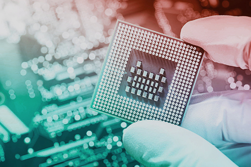
According to Nikkei Chinese website on April 20th, TSMC, the world's largest semiconductor foundry, has recently joined Japan's national project "Advanced Semiconductor Manufacturing Program Development".
It is reported that Japan officially launched the project in 2021, with the goal of "keeping semiconductor manufacturing technology in Japan". The project is participated by institutions such as the Japan Industrial Technology Research Institute, TEPCO Electronics, Canon, TSMC Japan 3DIC Research and Development Center, and the Advanced Systems Technology Research Group. It is expected to provide 76 billion yen in funding within five years. TSMC's research base in Japan, TSMC Japan 3DIC R&D Center, plans to jointly develop the 3D post-processing technology "3DIC" in semiconductor manufacturing with Japan.
It is reported that this project is part of the business promoted by the Japan New Energy Industry Technology Development Organization (NEDO) since 2019. The project is based on an industrial technology comprehensive research institute with the most advanced clean rooms, located in Tsukuba City, Ibaraki Prefecture. Enterprises and universities develop manufacturing technology for logic semiconductors here.
The semiconductor manufacturing process is divided into "pre process" and "post process". The former refers to the process of forming circuits on a silicon substrate using exposure equipment, while the latter refers to the process of assembling after segmentation. The project has also set research topics based on these two processes, with the common keyword being "three-dimensional (3D)".
Specifically, in terms of front-end processes, the project is committed to developing the most advanced component technology known as "nanosheets", and there are reports that 3D nanosheets will become mainstream after 2025. In terms of post-processing, this project will establish the technology of vertically stacked circuits. It should be noted that 3D integration is a powerful technology that breaks the limits of Moore's Law. Advanced packaging has recently received significant attention, especially through silicon via technology. 3D integration involves vertically stacking chips and utilizing advanced packaging technologies such as wafer level packaging and through silicon via to improve performance.